
Samsung and TSMC adopt ASML's new photomask technology to improve chip production
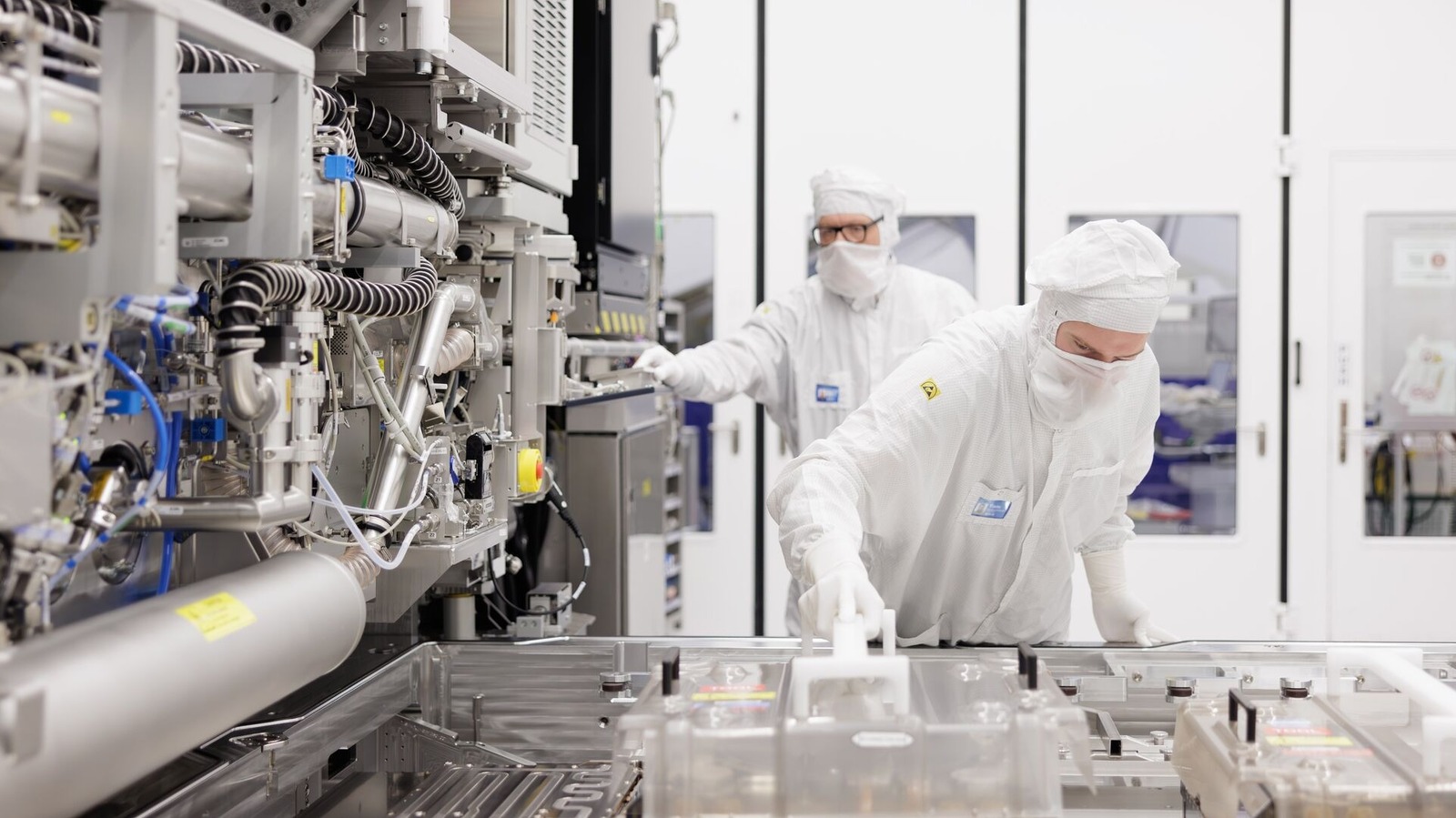
Semiconductor giants Samsung and TSMC are collaborating with ASML to implement larger chip photomasks in their manufacturing processes. This technological shift is designed to enhance production yields and reduce overall costs for advanced semiconductor fabrication. By utilizing these new machines, the companies aim to address ongoing supply chain challenges and improve the efficiency of chip production. The adoption of these larger photomasks represents a significant step forward in lithography technology, allowing for more complex patterns to be printed on silicon wafers with greater precision. As the demand for high-performance chips continues to grow across various industries, this partnership with ASML is expected to play a critical role in stabilizing the market and ensuring a more consistent supply of essential hardware components. This move highlights the industry's ongoing commitment to innovation as a primary solution to manufacturing bottlenecks.
This is a summary. Read the full article at the original source:
EngadgetRelated stories

Restarting your computer is a piece of advice that has persisted for decades, but its relevance in the modern computing landscape is often debated. Wh…

From Wearables to Robots to Tabletop Trinkets, the AI Hardware Scene Is Booming
At IFA 2026, the consumer electronics landscape showcased a significant shift toward dedicated AI hardware. Moving beyond software-based integrations,…

In a detailed technical breakdown, developer Nishant Joshi explores the complex engineering challenges involved in building a functional printer from…